
文章目录[隐藏]

VHDL简介
VHDL 的历史
VHDL 的 英 文 全 名 是 Very-High-Speed Integrated Circuit Hardware DescriptionLanguage,诞生于 1982 年。
1987 年底,VHDL 被 IEEE 和美国国防部确认为标准硬件描述语言。自 IEEE 公布了 VHDL 的标准版本 IEEE-1076(简称 87 版)之后,各 EDA 公司相继推出了自己的 VHDL 设计环境,或宣布自己的设计工具可以提供 VHDL 接口。此后 VHDL 在电子设计领域逐步取代了原有的各种非标准硬件描述语言。
1993 年,IEEE 对 VHDL 进行了修订,从更高的抽象层次和系统描述能力上扩展 VHDL 的内容,并公布了新版本的 VHDL,即 IEEE 标准的 1076-1993版本(简称 93 版)。
现在,VHDL 和 Verilog HDL 作为 IEEE 的工业标准硬件描述语言,在电子工程领域已成为事实上的通用硬件描述语言。
VHDL 的特点
VHDL 主要用于描述数字系统的结构、行为、功能和接口。除了含有许多具有硬件特征的语句外,VHDL 在语言形式、描述风格和句法上与一般的计算机高级语言十分相似。VHDL 的程序结构特点是将一项工程设计,或称设计实体(可以是一个元件、一个电路模块或一个系统)分成外部和内部两部分。
外部也可称为可视部分,它描述了此模块的端口,而内部可称为不可视部分,它涉及到实体的功能实现和算法完成。在对一个设计实体定义了外部端口后,一旦其内部开发完成,其他的设计就可以直接调用这个实体。这种将设计实体分成内外部分的概念是VHDL 系统设计的基本点。
应用 VHDL 进行工程设计有以下的优点:
1.行为描述
与其他的硬件描述语言相比,VHDL 具有更强的行为描述能力,强大的行为描述能力是避开具体的器件结构,从逻辑行为上描述和设计大规模电子系统的重要保证。
2.仿真模拟
VHDL 丰富的仿真语句和库函数,使得在任何系统的设计早期就能查验设计系统的功能可行性,随时可对设计进行仿真模拟。
3.大规模设计
一些大型的 FPGA 设计项目必须有多人甚至多个开发组共同并行工作才能实现。VHDL 语句的行为描述能力和程序结构决定了它具有支持大规模设计的分解和已有设计的再利用功能。
4.门级网表
对于用 VHDL 完成的一个确定的设计,可以利用 EDA 工具进行逻辑综合和优化,并自动把VHDL 描述设计转变成门级网表。
5.独立性
VHDL 对设计的描述具有相对独立性,设计者可以不懂硬件的结构,也不必对最终设计实现的目标器件有很深入地了解。
VHDL 程序基本结构
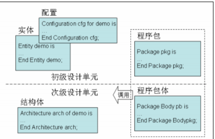
一般的 VHDL 程序可以由实体(Entity)、结构体(Architecture)、配置(Configuration)、程序包和程序包体(Package)以及库(Library)5 个部分组成,它们是 VHDL 程序的设计单元。
其中实体、配置和程序包属于初级设计单元,主要的功能是进行端口、行为、函数等的定义。结构体和程序包体是次级设计单元,包含了所有行为以及函数的实现代码。其中,程序包和程序包体又属于公用设计单元,即它们是被其他程序模块调用的。库则是一批程序包的集合。
图 1 所示为 VHDL 程序设计单元之间的关系。
设计思路
步骤
进行VHDL设计时,通常的设计逻辑思路可以分为以下几个步骤:
- 明确功能需求
- 首先需要明确你要设计的电路或系统的功能需求。这一步是最重要的,因为它决定了你后续所有设计工作的方向。
- 理解原理图(如果有)
- 如果有原理图,可以通过原理图来理解电路的工作原理。原理图可以帮助你直观地看到电路的连接和逻辑关系。
- 推导真值表
- 根据功能需求或原理图,推导出电路的真值表。真值表列出了所有可能的输入组合及其对应的输出结果。
- 对于组合逻辑电路,真值表是非常有用的工具,可以帮助你理解输入和输出之间的关系。
- 写出逻辑表达式
- 根据真值表,写出逻辑表达式。这些表达式描述了输出如何根据输入进行计算。
- 可以使用布尔代数、卡诺图等方法来简化逻辑表达式。
- 编写VHDL代码
- 根据逻辑表达式,编写VHDL代码。VHDL代码描述了电路的行为和结构。
- 在编写代码时,需要定义实体(Entity)和架构(Architecture)。实体定义了电路的接口(输入和输出端口),架构定义了电路的具体实现。
- 仿真和验证
- 编写测试平台(Testbench),对VHDL代码进行仿真和验证。测试平台用于模拟输入信号,并检查输出信号是否符合预期。
- 通过仿真,可以发现并修正设计中的错误。
- 综合和实现
- 将经过验证的VHDL代码综合成具体的硬件描述(如门级网表)。
- 进行布局布线,将设计映射到具体的FPGA或ASIC上。
- 硬件测试
- 将设计下载到FPGA或ASIC上进行硬件测试,确保设计在实际硬件上能够正常工作。
总结来说,VHDL设计的逻辑思路通常是:
- 明确功能需求。
- 理解原理图(如果有)。
- 推导真值表。
- 写出逻辑表达式。
- 编写VHDL代码。
- 仿真和验证。
- 综合和实现。
- 硬件测试。
逻辑表达式推导
通过真值表推导逻辑表达式的过程可以分为以下几个步骤:
- 列出真值表
- 首先,列出所有输入变量的所有可能组合,以及每种组合对应的输出结果。
- 找出输出为1的行
- 在真值表中,找出所有输出为1的行。这些行对应的输入组合将用于构建逻辑表达式。
- 写出每一行的最小项(Minterm)
- 对于每一行输出为1的输入组合,写出一个最小项(Minterm)。最小项是输入变量的与(AND)组合,其中输入为0的变量取反(NOT),输入为1的变量保持不变。
- 将所有最小项相或(OR)
- 将所有最小项相或(OR)起来,得到最终的逻辑表达式。
示例:全加器的Sum输出
假设我们有一个全加器的真值表,如下所示:
| a | b | cin | Sum (so) | Carry (co) |
| 0 | 0 | 0 | 0 | 0 |
| 0 | 0 | 1 | 1 | 0 |
| 0 | 1 | 0 | 1 | 0 |
| 0 | 1 | 1 | 0 | 1 |
| 1 | 0 | 0 | 1 | 0 |
| 1 | 0 | 1 | 0 | 1 |
| 1 | 1 | 0 | 0 | 1 |
| 1 | 1 | 1 | 1 | 1 |
我们要推导出Sum(so)的逻辑表达式。
- 找出输出为1的行
- 输出Sum为1的行是:
- a=0, b=0, cin=1
- a=0, b=1, cin=0
- a=1, b=0, cin=0
- a=1, b=1, cin=1
- 写出每一行的最小项
- 对于a=0, b=0, cin=1,最小项是a’b’cin
- 对于a=0, b=1, cin=0,最小项是a’bcin’
- 对于a=1, b=0, cin=0,最小项是ab’cin’
- 对于a=1, b=1, cin=1,最小项是abc
- 将所有最小项相或
- 最终的逻辑表达式是:
Sum = a'b'cin + a'bcin' + ab'cin' + abcCode language: JavaScript (javascript)示例:全加器的Carry输出
同样,我们可以推导出Carry(co)的逻辑表达式。
- 找出输出为1的行
- 输出Carry为1的行是:
- a=0, b=1, cin=1
- a=1, b=0, cin=1
- a=1, b=1, cin=0
- a=1, b=1, cin=1
- 写出每一行的最小项
- 对于a=0, b=1, cin=1,最小项是a’bcin
- 对于a=1, b=0, cin=1,最小项是ab’cin
- 对于a=1, b=1, cin=0,最小项是abc’in
- 对于a=1, b=1, cin=1,最小项是abc
- 将所有最小项相或
- 最终的逻辑表达式是:
Carry = a'bcin + ab'cin + abc'in + abcCode language: JavaScript (javascript)简化逻辑表达式
在得到逻辑表达式后,可以使用布尔代数或卡诺图(Karnaugh Map)等方法对表达式进行简化。例如,对于全加器的Sum输出,可以简化为:
Sum = a XOR b XOR cinCode language: PHP (php)对于全加器的Carry输出,可以简化为:
Carry = (a AND b) OR (b AND cin) OR (a AND cin)卡诺图(Karnaugh Map)
卡诺图是一种图形化的方法,用于简化逻辑表达式。通过将真值表中的信息映射到卡诺图上,可以直观地找到最小项并进行合并,从而得到简化的逻辑表达式。
卡诺图的步骤
- 绘制卡诺图
- 根据输入变量的数量绘制卡诺图。对于n个输入变量,卡诺图有2^n个格子。
- 填写真值表
- 将真值表中的输出结果填入卡诺图的相应格子中。
- 合并最小项
- 在卡诺图中找到相邻的1,并将它们合并成更大的组。每个组代表一个简化的最小项。
- 写出简化表达式
- 根据合并后的组,写出简化的逻辑表达式。
示例:简化全加器的Sum输出
全加器的Sum输出逻辑表达式为:
Sum = a'b'cin + a'bcin' + ab'cin' + abcCode language: JavaScript (javascript)- 绘制卡诺图
| ab\cin | 0 | 1 |
| 00 | 0 | 1 |
| 01 | 1 | 0 |
| 11 | 0 | 1 |
| 10 | 1 | 0 |
- 填写真值表
| ab\cin | 0 | 1 |
| 00 | 0 | 1 |
| 01 | 1 | 0 |
| 11 | 0 | 1 |
| 10 | 1 | 0 |
- 合并最小项
- 合并相邻的1,得到两个组:
- 组1:a’b’cin 和 a’bcin’
- 组2:ab’cin’ 和 abc
- 写出简化表达式
- 组1:a XOR b XOR cin
- 组2:a XOR b XOR cin
最终简化结果为:
Sum = a XOR b XOR cinCode language: PHP (php)电路设计
组合逻辑电路
基本逻辑门
二端输入或门ORR2
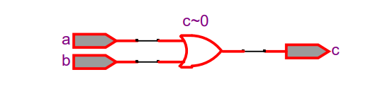
--逻辑 OR 门的功能模块
LIBRARY IEEE;
USE IEEE.STD_LOGIC_1164.ALL;

--定义了一个名为 orr2 的实体(Entity)
ENTITY orr2 IS
    PORT(
        a, b: IN STD_LOGIC;    --输入端口 a 和 b
        c: OUT STD_LOGIC    --输出端口 c
    );
END ENTITY orr2;

--定义了一个名为 full 的架构(Architecture)它实现了 orr2 实体的行为
ARCHITECTURE ful OF orr2 IS
BEGIN
    c <= a OR b;  -- c 总是等于 a 和 b 的逻辑 OR 值
END ARCHITECTURE ful;Code language: PHP (php)
反相器
library ieee;
use ieee.std_logic_1164.all;

entity not is
    port(
        a:in std_logic;
        y:out std_logic);
end not;

architecture behave of not is
begin
    y<= not a;
end behave;Code language: PHP (php)
与非门
使用并行语句、逻辑运算符描述;
library ieee;
use ieee.std_logic_1164.all;

entity nand2 is
port(
    a,b:in std_logic;
     y:out std_logic);
end nand2;

architecture behave1 of nand2 is
begin
    y<=a nand b;
end behave1;Code language: PHP (php)
用进程语句描述之一
architecture behave2 of nand2 is
begin
    process(a,b)
    begin
    y<=a nand b;
    end process;
end behave2;
用进程语句描述之二;
architecture behave3 of nand2 is
begin
    process(a,b)
    begin
        if a=‘1’ and b=‘1’ then
            y<=‘0’;
        else
            y<=‘1’;
        end if;
    end process;
end behave3;Code language: JavaScript (javascript)
用进程语句描述之三;
architecture behave4 of nand2 is
signal sel:std_logic_vector(1 downto 0);
begin
    sel=a &b;
    process(sel)
    begin
        case sel is
            when “11” => y<=‘0’;
            when “10” => y<=‘1’;
            when “01” => y<=‘1’;
            when “00” => y<=‘1’;
            when others => y<=‘X’;
            end case;
     end process;
end behave4;Code language: PHP (php)
求补器
Library ieee;
Use ieee.std_logic_1164.all;
Use ieee.std_logic_unsigned.all;
Entity complementer is
    generic(delay_multiply,delay_done:time);
    port(
        a:in std_logic_vector(7 downto 0);
        b:out std_logic_vector(7 downto 0));
End complementer;

Architecture arc of complemente is
    Begin
    B<=not a+’1’;
End arc;Code language: PHP (php)
数据选择器和分配器
四选一数据选择器
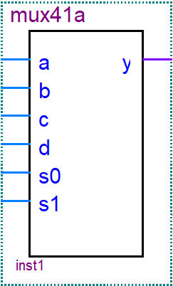
library ieee;
use ieee.std_logic_1164.all;

-- 定义一个4-to-1数据选择器(MUX)
entity mux41a is
    Port (
        a, b, c, d : in std_logic; -- 四个输入信号
        s0, s1 : in std_logic; -- 两个选择信号
        y : out std_logic -- 输出信号
    );
end mux41a;

-- RTL(Register Transfer Level)架构实现
architecture rtl of mux41a is
    -- 定义一个2位的信号向量,用于存储s1和s0的选择信号
    signal s : std_logic_vector(1 downto 0);
begin
    -- 合并s1和s0为一个2位向量
    s <= s1 & s0;

    -- 过程:根据选择信号s的值,确定输出y的值
    process(s1, s0)
    begin
        -- 用case语句根据选择信号的组合,选择对应的输入信号作为输出
        case s is
            when "00" => y <= a; -- 当s为00时,输出a
            when "01" => y <= b; -- 当s为01时,输出b
            when "10" => y <= c; -- 当s为10时,输出c
            when "11" => y <= d; -- 当s为11时,输出d
            when others => y <= '0'; -- 其他情况,输出低电平
        end case;
    end process;
end rtl;Code language: PHP (php)
八选一数据选择器
library ieee;
use ieee.std_logic_1164.all;

-- 定义一个8选1数据选择器(MUX)
entity mux8_1 is
    Port (
        input : in std_logic_vector(7 downto 0); -- 8位输入数据
        a, b, c : in std_logic; -- 3位选择信号
        y : out std_logic -- 输出数据
    );
end mux8_1;

-- RTL(寄存器传输级)实现架构
architecture rtl of mux8_1 is
    -- 定义一个3位的信号用于内部选择逻辑
    signal sel : std_logic_vector(2 downto 0);
begin
    -- 将选择信号a, b, c连接到内部选择信号sel
            sel <= a & b & c;

    -- 过程:根据选择信号sel,设置输出y
process(input, sel)
        begin
    if (sel = "000") then
        y <= input(0);
    elsif(sel = "001") then
        y <= input(1);
    elsif(sel = "010") then
        y <= input(2);
    elsif(sel = "011") then
        y <= input(3);
    elsif(sel = "100") then
        y <= input(4);
    elsif(sel = "101") then
        y <= input(5);
    elsif(sel = "110") then
        y <= input(6);
    else
        y <= input(7);
    end if;
end process;
end rtl;Code language: PHP (php)
数据分配器
library ieee;
use ieee.std_logic_1164.all;
-- 引入IEEE标准库和标准逻辑1164库

entity demux8 is
port(
    a, b, c : in std_logic; -- 输入端口 a, b, c,标准逻辑类型
    y : in std_logic; -- 输入信号 y,标准逻辑类型
    input : out std_logic_vector(7 downto 0) -- 输出端口 input,8位宽的标准逻辑向量
);
end demux8;
-- 定义一个8路解复用器实体

architecture rtl of demux8 is
signal sel : std_logic_vector(2 downto 0);
-- 定义内部信号 sel,3位宽的标准逻辑向量
begin
sel <= a & b & c;
-- 将输入 a, b, c 连接成一个3位的向量赋值给 sel

process(y, sel)
begin
    case sel is
        when "000" => input(0) <= y; -- 当 sel 为 "000" 时,将 y 赋值给 input(0)
        when "001" => input(1) <= y; -- 当 sel 为 "001" 时,将 y 赋值给 input(1)
        when "010" => input(2) <= y; -- 当 sel 为 "010" 时,将 y 赋值给 input(2)
        when "011" => input(3) <= y; -- 当 sel 为 "011" 时,将 y 赋值给 input(3)
        when "100" => input(4) <= y; -- 当 sel 为 "100" 时,将 y 赋值给 input(4)
        when "101" => input(5) <= y; -- 当 sel 为 "101" 时,将 y 赋值给 input(5)
        when "110" => input(6) <= y; -- 当 sel 为 "110" 时,将 y 赋值给 input(6)
        when "111" => input(7) <= y; -- 当 sel 为 "111" 时,将 y 赋值给 input(7)
        when others => input <= "XXXXXXXX"; -- 其他情况下,将 input 赋值为 "XXXXXXXX"
    end case;
end process;
-- 使用case语句根据sel的值设置input的值,实现解复用功能

end rtl;
-- 定义8路解复用器的结构体Code language: PHP (php)
LIBRARY IEEE; USE IEEE.STD_LOGIC_1164.ALL;
USE IEEE.STD_LOGIC_UNSIGNED.ALL;
ENTITY traffic IS
PORT (clk:in std_logic;
led7s1:out std_logic_vector(6 downto 0);
led7s2:out std_logic_vector(6 downto 0);
comb_out:out std_logic_vector(5 downto 0));
END;
ARCHITECTURE one OF traffic IS
TYPE dm IS (s0,s1,s2,s3);
SIgnal current_state,next_state:dm;
SIGNAL FULL : STD_LOGIC;
SIGNAL tl :STD_LOGIC_VECTOR(6 DOWNTO 0);
SIGNAL th:STD_LOGIC_VECTOR(1 DOWNTO 0);
SIGNAL tm :STD_LOGIC_VECTOR(6 DOWNTO 0);
SIGNAL TIME :STD_LOGIC_VECTOR(6 DOWNTO 0);
BEGIN
P_REG: PROCESS(CLK)
VARIABLE CNT8:STD_LOGIC_VECTOR(7 DOWNTO 0);
BEGIN
IF CLK'EVENT AND CLK='1' THEN
IF CNT8 = "11111111" THEN
CNT8:="01111111";
FULL<='1';
ELSE CNT8 := CNT8+1;
FULL <= '0';
END IF;
END IF;
END PROCESS P_REG;
PROCESS(full)
BEGIN
IF full'EVENT AND full='1' THEN
IF TIME<"1000011" THEN
TIME<=TIME+1;
ELSe TIME <="0000000";
END IF;
END IF;
END PROCESS;
REG:process( full,current_state)
BEGIN
IF full='1' AND full'EVENT THEN
current_state<=next_state;
END IF;
END process;
COM:process(current_state, time)
begin
case current_state is
when s0=>comb_out<="001100";tm<=39-time;
if time=39 then next_state<=s1;
else next_state<=s0;
end if;
when s1=>comb_out<="010100";tm<=43-time;
if time=43 then next_state<=s2;
else next_state<=s1;
end if;
when s2=>comb_out<="100010";tm<=63-time;
if time=63 then next_state<=s3;
else next_state<=s2;
end if;
when s3=>comb_out<="100001";tm<=67-time;
if time=67 then next_state<=s0;
else next_state<=s3;
end if;
end case;
end process;
PROCESS(tm)
BEGIN
IF tm>=30 THEN th<="11";tl<=tm-30;
ELSIF tm>=20 THEN th<="10";tl<=tm-20;
ELSIF tm>=10 THEN th<="01";tl<=tm-10;
ELSE th<="00";tl<=tm;
END IF;
END PROCESS;
process(th,tl)
begin
case th is
when"00"=>led7s1<="0111111";
when"01"=>led7s1<="0000110";
when"10"=>led7s1<="1011011";
when"11"=>led7s1<="1001111";
when others=>null;
end case;
case tl is
when "0000000"=>led7s2<="0111111";
when "0000001"=>led7s2<="0000110";
when "0000010"=>led7s2<="1011011";
when "0000011"=>led7s2<="1001111";
when"0000100"=>led7s2<="1100110";
when "0000101"=>led7s2<="1101101";
when "0000110"=>led7s2<="1111101";
when"0000111"=>led7s2<="0000111";
when "0001000"=>led7s2<="1111111";
when "0001001"=>led7s2<="1101111";
when others=>null;
end case;
end process;
end; Code language: PHP (php)译码器和编码器
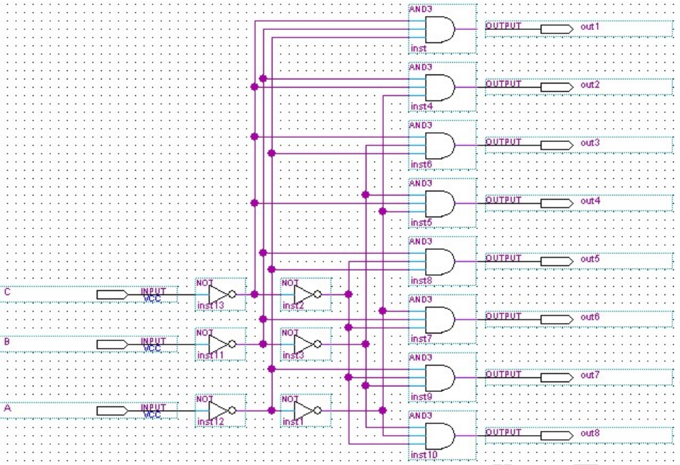
三-八译码器
三八译码器(3-to-8 Decoder)是一种数字电路,它将3位二进制输入信号转换为8个独立的输出信号。具体来说,三八译码器有3个输入端和8个输出端。根据输入端的不同组合,译码器会激活其中一个输出端,而其他输出端保持不变。
工作原理
三八译码器的输入端通常标记为A、B、C,输出端标记为Y0到Y7。输入端的3位二进制数可以表示8种不同的组合(从000到111),每种组合对应一个唯一的输出端被激活。例如,当输入为000时,输出Y0被激活;当输入为001时,输出Y1被激活;依此类推。
真值表
以下是真值表,展示了三八译码器的输入与输出之间的关系:
| 输入A | 输入B | 输入C | 输出Y0 | 输出Y1 | 输出Y2 | 输出Y3 | 输出Y4 | 输出Y5 | 输出Y6 | 输出Y7 |
| 0 | 0 | 0 | 1 | 0 | 0 | 0 | 0 | 0 | 0 | 0 |
| 0 | 0 | 1 | 0 | 1 | 0 | 0 | 0 | 0 | 0 | 0 |
| 0 | 1 | 0 | 0 | 0 | 1 | 0 | 0 | 0 | 0 | 0 |
| 0 | 1 | 1 | 0 | 0 | 0 | 1 | 0 | 0 | 0 | 0 |
| 1 | 0 | 0 | 0 | 0 | 0 | 0 | 1 | 0 | 0 | 0 |
| 1 | 0 | 1 | 0 | 0 | 0 | 0 | 0 | 1 | 0 | 0 |
| 1 | 1 | 0 | 0 | 0 | 0 | 0 | 0 | 0 | 1 | 0 |
| 1 | 1 | 1 | 0 | 0 | 0 | 0 | 0 | 0 | 0 | 1 |
应用
三八译码器在数字电路中有广泛的应用,主要用于以下几个方面:
- 地址解码:在存储器中,根据地址选择特定的存储单元。
- 数据选择:在多路复用器中,根据选择信号选择特定的数据输入。
- 控制信号生成:在控制单元中,根据输入信号生成特定的控制信号。
原理图
VHDL
-- 解码器实体声明
library IEEE;
use IEEE.std_logic_1164.all;
-- 引入IEEE标准库和标准逻辑1164库

entity decoder3 is
    -- 输入和输出端口声明
    port(
        A, B, C : in STD_LOGIC; -- 输入端口 A, B, C,标准逻辑类型
        OUT1, OUT2, OUT3, OUT4, OUT5, OUT6, OUT7, OUT8 : out STD_LOGIC -- 输出端口 OUT1 到 OUT8,标准逻辑类型
    );
end decoder3;
-- 定义一个3位输入的解码器实体

-- 解码器架构定义
architecture decoder3_arch of decoder3 is
    -- 定义内部信号K,用于根据输入A, B, C的组合进行解码
    signal K : STD_LOGIC_VECTOR(2 downto 0); -- 内部信号 K,3位宽的标准逻辑向量
    -- 定义内部信号POUT,用于存储解码后的输出状态
    signal POUT : STD_LOGIC_VECTOR(7 downto 0); -- 内部信号 POUT,8位宽的标准逻辑向量
begin
    -- 将输入A, B, C连接到信号K,为后续的case语句做准备
    K <= C & B & A; -- 将输入 C, B, A 连接成一个3位的向量赋值给 K

    -- 根据信号K的值,设置POUT的值,实现解码功能
    process(K)
    begin
        case K is
            when "000" => POUT <= "00000001"; -- 当 K 为 "000" 时,POUT 为 "00000001"
            when "001" => POUT <= "00000010"; -- 当 K 为 "001" 时,POUT 为 "00000010"
            when "010" => POUT <= "00000100"; -- 当 K 为 "010" 时,POUT 为 "00000100"
            when "011" => POUT <= "00001000"; -- 当 K 为 "011" 时,POUT 为 "00001000"
            when "100" => POUT <= "00010000"; -- 当 K 为 "100" 时,POUT 为 "00010000"
            when "101" => POUT <= "00100000"; -- 当 K 为 "101" 时,POUT 为 "00100000"
            when "110" => POUT <= "01000000"; -- 当 K 为 "110" 时,POUT 为 "01000000"
            when others => POUT <= "10000000"; -- 其他情况下,POUT 为 "10000000"
        end case;
    end process;
    -- 使用case语句根据K的值设置POUT的值,实现解码功能

    -- 将POUT信号的各个位连接到对应的输出端口
    OUT1 <= POUT(0); -- 将 POUT 的第0位连接到输出端口 OUT1
    OUT2 <= POUT(1); -- 将 POUT 的第1位连接到输出端口 OUT2
    OUT3 <= POUT(2); -- 将 POUT 的第2位连接到输出端口 OUT3
    OUT4 <= POUT(3); -- 将 POUT 的第3位连接到输出端口 OUT4
    OUT5 <= POUT(4); -- 将 POUT 的第4位连接到输出端口 OUT5
    OUT6 <= POUT(5); -- 将 POUT 的第5位连接到输出端口 OUT6
    OUT7 <= POUT(6); -- 将 POUT 的第6位连接到输出端口 OUT7
    OUT8 <= POUT(7); -- 将 POUT 的第7位连接到输出端口 OUT8
end decoder3_arch;
-- 定义解码器的结构体Code language: PHP (php)
7 段 LED 译码显示器
七段数码管可以用来显示十进制数码,见图 3-2。它包含有七个笔划,通过控制各笔划的亮暗显示出数字。它的输入信号端(a, b, c, d, e, f, g)与显示数码(十进制数字)的对应关系如表 3-2 所示。对应的七段译码器电路图如图 3-3 所示。其输入为代表显示数字的二进制数(BCD 码 x4, x3, x2, x1),输出为数码管的输入信号。


VHDL
LIBRARY IEEE;
USE IEEE.STD_LOGIC_1164.ALL;

ENTITY DECL7S IS
    PORT (
        X : IN STD_LOGIC_VECTOR(3 DOWNTO 0);
        LED7S : OUT STD_LOGIC_VECTOR(6 DOWNTO 0)
    );
END DECL7S;

ARCHITECTURE ONE OF DECL7S IS
BEGIN
    PROCESS(X)
    BEGIN
        CASE X IS
            WHEN "0000" => LED7S <= "0111111";
            WHEN "0001" => LED7S <= "0000110";
            WHEN "0010" => LED7S <= "1011011";
            WHEN "0011" => LED7S <= "1001111";
            WHEN "0100" => LED7S <= "1100110";
            WHEN "0101" => LED7S <= "1101101";
            WHEN "0110" => LED7S <= "1111101";
            WHEN "0111" => LED7S <= "0000111";
            WHEN "1000" => LED7S <= "1111111";
            WHEN "1001" => LED7S <= "1101111";
            WHEN "1010" => LED7S <= "1110111";
            WHEN "1011" => LED7S <= "1111100";
            WHEN "1100" => LED7S <= "0111001";
            WHEN "1101" => LED7S <= "1011110";
            WHEN "1110" => LED7S <= "1111001";
            WHEN "1111" => LED7S <= "1110001";
            WHEN OTHERS => NULL;
        END CASE;
    END PROCESS;
END ONE; Code language: PHP (php)
八-三优先编码器设计
library ieee;
use ieee.std_logic_1164.all;
entity encoder3 is
 port ( a, b, c, d, e, f, g, h : in std_logic;
 out2, out1, out0 : out std_logic);
end encoder3;
architecture behave of encoder3 is
signal k:std_logic_vector(2 downto 0);
begin
 process (a, b, c, d, e, f, g, h)
 begin
 if ( a='0') then
 k<= "000";
 elsif( b='0') then
 k<= "001";
 elsif( c='0') then
 k<= "010";
 elsif( d='0') then
 k<= "011";
 elsif( e='0') then
 k<= "100";
 elsif( f='0') then
 k<= "101";
 elsif( g='0') then
 k<= "110";
 else-------------------------注意此处的特点及用法。
 k<= "111";
 end if;
out2<=k(2);
out1<=k(1);
out0<=k(0);
end process;
end behave; Code language: PHP (php)
比较器
1、描述之一:

library ieee;
use ieee.std_logic_1164.all;

entity comparator is
    port(
        in1, in2:in std_logic_vector(3 downto 0);
        g, e, l:out std_logic);
end comparator;

architecture arc of comparator is
    signal temp:std_logic_vector(2 downto 0);
    begin
    process(in1, in2)
    begin
        if in1>in2 then
            temp<="100";
        elsif in1< in2 then
            temp<="001";
        else
            temp<="010";
        end if;
    g<=temp(2); e<=temp(1);l<=temp(0);
    end process;
end arc;Code language: PHP (php)
2、比较器的另一种描述:
library ieee;
use ieee.std_logic_1164.all;
use ieee.std_logic_unsigned.all;
entity comparator is
port(in1, in2:in std_logic_vector(3 downto 0);
g, e, l:out std_logic);
end comparator;
architecture arc2 of comparator is
begin
process(in1, in2)
begin
if in1>in2 then
g<=‘1’; e<=‘0’; l<=‘0’;
elsif in1=in2 then
g<=‘0’; e<=‘1’; l<=‘0’;
else
g<=‘0’; e<=‘0’; l<=‘1’;
end if;
end process;
end arc2;Code language: PHP (php)
乘法器
实现乘(除)法的方法:
(1)用软件编程;
(2)在加法器、移位器的基础上适当增
加一些硬件;
(3)设置专用乘除法部件。
用加法器、移位器实现乘法器:
Library ieee;
Use ieee.std_logic_1164.all;
Use ieee.std_logic_unsigned.all;
Entity mult is
generic(delay_multiply,delay_done:time);
port(in1, in2:in std_logic_vector(3 downto 0);
product:out std_logic_vector(7 downto 0));
End mult;
Architecture arc of mult is
Begin
process(in1,in2)
variable acc,shift:std_logic_vector(7 downto 0);
variable temp:std_logic_vector(3 downto 0);
begin
acc:=(others=>'0');
temp:=(others=>'0'); shift:=temp & in1;
for i in 0 to 3 loop
if in2(i)='1' then
acc:=acc+shift;
end if;
shift:=shift(6 downto 0) & '0';
end loop;
product<=acc;
end process;
End arc;Code language: PHP (php)
用加法器、移位寄存器实现乘法器:
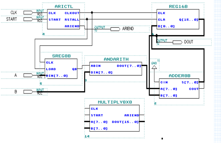
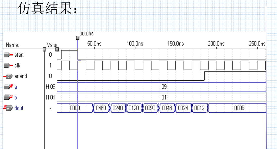
顶层模块:
library ieee;
use ieee.std_logic_1164.all;

entity multiply8x8 is
    port(
    clk,start:in std_logic;
    a,b:in std_logic_vector(7 downto 0);
    ariend:out std_logic;
    dout:out std_logic_vector(15 downto 0));
end multiply8x8;

architecture struc of multiply8x8 is
component arictl
    port(
        clk,start:in std_logic;
        clkout,rstall:out std_logic);
        ariend:out std_logic);
end component;

component andarith
    port(
        abin:in std_logic;
        din:in std_logic_vector(7 downto 0);
        dout:out std_logic_vector(7 downto 0));
end component;

component adder8b1
    PORT (
        CIN:IN STD_LOGIC;
        A :IN STD_LOGIC_VECTOR(7 DOWNTO 0);
        B :IN STD_LOGIC_VECTOR(7 DOWNTO 0);
        S:OUT STD_LOGIC_VECTOR(7 DOWNTO 0);
        COUT7:OUT STD_LOGIC);
end component;

component sreg8b
    port(
        clk,load:in std_logic;
        din:in std_logic_vector(7 downto 0);
        qb:out std_logic);
    end component;

component reg16b
    port(
        clk,clr:in std_logic;
        d:in std_logic_vector(8 downto 0);
        q:out std_logic_vector(15 downto 0));
end component;

signal gndint:std_logic;
signal intclk:std_logic;
signal rstall:std_logic;
signal qb:std_logic;
signal andsd:std_logic_vector(7 downto 0);
signal dtbin:std_logic_vector(8 downto 0);
signal dtbout:std_logic_vector(15 downto 0);

begin
    dout<=dtbout;
    gndint<='0';
    u1:arictl port map(clk,start,intclk,rstall,ariend);
    u2:sreg8b port map(intclk,rstall,b,qb);
    u3:andarith port map(qb,a,andsd);
    u4:adder8b1 port map(gndint,dtbout(15 downto8),andsd,dtbin(7 downto 0),dtbin(8));
    u5:reg16b port map(intclk,rstall,dtbin,dtbout);
end struc;Code language: PHP (php)
ADDER8B 模块:
LIBRARY IEEE;
USE IEEE.STD_LOGIC_1164.ALL;
USE IEEE.STD_LOGIC_UNSIGNED.ALL;
ENTITY ADDER8B IS
PORT (CIN:IN STD_LOGIC;
A :IN STD_LOGIC_VECTOR(7 DOWNTO 0);
B :IN STD_LOGIC_VECTOR(7 DOWNTO 0);
SUM:OUT STD_LOGIC_VECTOR(7 DOWNTO 0);
COUT:OUT STD_LOGIC);
END ADDER8B;
ARCHITECTURE STRUC OF ADDER8B IS
COMPONENT ADD4BIT
PORT(CIN:IN STD_LOGIC;
A4:IN STD_LOGIC_VECTOR(3 DOWNTO 0);
B4:IN STD_LOGIC_VECTOR(3 DOWNTO 0);
SUM4:OUT STD_LOGIC_VECTOR
(3 DOWNTO 0);
COUT4:OUT STD_LOGIC);
END COMPONENT;
SIGNAL CARRY_OUT:STD_LOGIC;
BEGIN
U1:ADD4BIT
PORT MAP(CIN=>CIN,
A4=>A(3 DOWNTO 0),
B4=>B(3 DOWNTO 0),
SUM4=>SUM(3 DOWNTO 0),
COUT4=>CARRY_OUT);
U2:ADD4BIT
PORT MAP(CIN=>CARRY_OUT,
A4=>A(7 DOWNTO 4),
B4=>B(7 DOWNTO 4),
SUM=>SUM(7 DOWNTO 4),
COUT4=>COUT);
END STRUC;Code language: PHP (php)
arictl模块:
library ieee;
use ieee.std_logic_1164.all;
use ieee.std_logic_unsigned.all;
entity arictl is
port(clk,start:in std_logic;
clkout,rstall:out std_logic;
ariend:out std_logic);
end arictl;
architecture behav of arictl is
signal cnt4b:std_logic_vector(3 downto 0);
begin
rstall<=start;
process(clk,start)
begin
if start='1' then
cnt4b<="0000";
elsif clk'event and clk='1' then
if cnt4b<8 then
cnt4b<=cnt4b+1;
end if;
end if;
end process;
process(clk,cnt4b,start)
begin
if start='0' then
if cnt4b<8 then
clkout<=clk;ariend<='0';
else
clkout<='0';ariend<='1';
end if;
else
clkout<=clk;ariend<='0';
end if;
end process;
end behav;Code language: PHP (php)
sreg8b模块:
library ieee;
use ieee.std_logic_1164.all;
entity sreg8b is
port(clk,load:in std_logic;
din:in std_logic_vector(7 downto 0);
qb:out std_logic);
end sreg8b;
architecture behav of sreg8b is
signal reg8: std_logic_vector(7 downto 0);
begin
process(clk,load)
begin
if clk'event and clk='1' then
if load='1' then
reg8<=din;
else
reg8(6 downto 0)<=reg8(7 downto 1);
end if;
end if;
end process;
qb<=reg8(0);
end behav;Code language: PHP (php)
reg16b模块:
library ieee;
use ieee.std_logic_1164.all;
entity reg16b is
port(clk,clr:in std_logic;
d:in std_logic_vector(8 downto 0);
q:out std_logic_vector(15 downto 0));
end reg16b;
architecture behav of reg16b is
signal r16s:std_logic_vector(15 downto 0);
begin
process(clk,clr)
begin
if clr='1' then
r16s<="0000000000000000";
elsif clk'event and clk='1' then
r16s(6 downto 0)<=r16s(7 downto 1);
r16s(15 downto 7)<=d;
end if;
end process;
q<=r16s;
end behav;Code language: PHP (php)
andarith模块;
library ieee;
use ieee.std_logic_1164.all;
entity andarith is
port(abin:in std_logic;
din:in std_logic_vector(7 downto 0);
dout:out std_logic_vector(7 downto 0));
end andarith;
architecture behav of andarith is
begin
process(abin,din)
begin
for i in 0 to 7 loop
dout(i)<=din(i) and abin;
end loop;
end process;
end behav;Code language: PHP (php)
缓冲器
单向总线缓冲器
library ieee;
use ieee.std_logic_1164.all;

entity tri_buffer8 is
    port(
    din:in std_logic_vector(7 downto 0);
    en:    in std_logic;
    dout:out std_logic_vector(7 downto 0));
end tri_buffer8;

architecture behave of tri_buffer8 is
begin
    process(din,en)
    begin
    case en is
        when '1'=>dout<=din;
        when others=>dout<=?ZZZZZZZZ";
    end case;
    end process;
end behave;Code language: PHP (php)
三态门电路
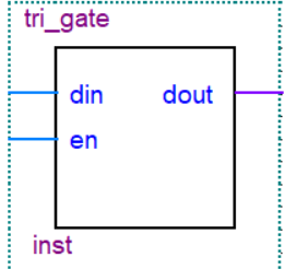
IF语句描述
library ieee;
use ieee.std_logic_1164.all;

entity tri_gate is
    port(
        din,en:in std_logic;
        dout:out std_logic);
end tri_gate ;

architecture behave1 of tri_gate is
begin
    process(din,en)
    begin
        if en=‘1’ then --可用case语句
            dout<=din; --描述
        else
            dout<=‘Z’;
        end if;
    end process;
end behave1;Code language: PHP (php)
case语句描述:
architecture behave2 of tri_gate is
begin
    process(din,en)
    begin
        case en is
            when ‘1’ => dout<=din;
            when others => dout<=‘Z’;
        end case;
    end process;
end behave2;Code language: PHP (php)
双向总线缓冲器
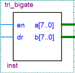
library ieee;
use ieee.std_logic_1164.all;

entity tri_bigate is
    port(
        a,b:inout std_logic_vector(7 downto 0);
        en:in std_logic;
        dr:in std_logic);
end tri_bigate;

architecture rtl of tri_bigate is
    signal aout,bout:std_logic_vector(7 downto 0);
    begin
    process(a, dr, en)
    begin
        if en='0' and dr='1' then
            bout<=a;
        else
            bout<="ZZZZZZZZ";
        end if;
    b<=bout;
    end process;

    process(b, dr, en)
    begin
        if en='0' and dr='0' then
            aout<=b;
        else
            aout<="ZZZZZZZZ";
        end if;
    a<=aout;
    end process;
end rtl;Code language: PHP (php)
移位器
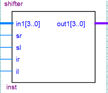
library ieee;
use ieee.std_logic_1164.all;

entity shifter is
    port(
        in1:in std_logic_vector(3 downto 0);
        sr, sl, ir, il : in std_logic;
        out1:out std_logic_vector(3 downto 0));
end shifter;

architecture arc of shifter is
    begin
    process(in1,sr,sl,ir,il)
        variable temp:std_logic_vector(0 to 1);
        begin
            temp:=sr & sl;
            case temp is
            when "00"=>out1<=in1;
            when "01"=>out1<=in1(2 downto 0)&il ;
            when "10"=>out1<=ir&in1(3 downto 1);
            when "11"=>out1<=in1;
            when others=>null;
            end case;
    end process;
end arc;Code language: PHP (php)
运算器
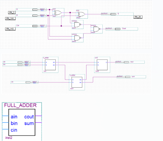
全加器
一位全加器
- 全加器的功能是将三个输入位(ain、bin、cin)相加,产生一个和位(sum)和一个进位位(cout)。
- 全加器可以通过两个半加器和一个或门来实现。第一个半加器处理两个输入位,第二个半加器处理第一个半加器的和位和第三个输入位,最后通过或门处理两个半加器的进位。
原理图1
真值表
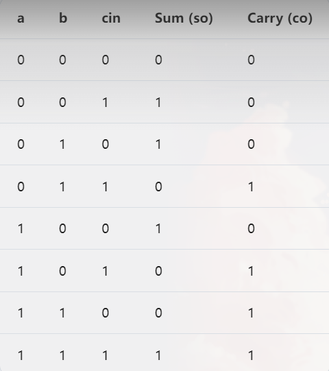
逻辑表达式
- sum = (ain XOR bin) XOR cin
- cout = (ain AND bin) OR ((ain XOR bin) AND cin)
Code language: PHP (php)
VHDL
--全加器--
--通过实例化两个半加器(h_adder)和一个或门(orr2)来实现全加器的功能
--全加器的设计使用了两个半加器和两个进位(一个来自第一个半加器,一个来自或门),以计算三个输入位?
LIBRARY IEEE;  -- 引入IEEE标准库
USE IEEE.STD_LOGIC_1164.ALL;  -- 使用IEEE标准逻辑1164库

ENTITY FULL_ADDER IS  -- 定义实体FULL_ADDER
    PORT(
        ain, bin, cin : IN STD_LOGIC;  -- 输入端口ain, bin, cin,类型为STD_LOGIC
        cout, sum     : OUT STD_LOGIC  -- 输出端口cout, sum,类型为STD_LOGIC
    );
END ENTITY FULL_ADDER;

-- 定义名为fd1的架构
ARCHITECTURE fd1 OF FULL_ADDER IS
    -- 定义了一个名为h_adder的半加器组件,它有两个输入端口a和b,以及两个输出端口co(进位)和so(和)
    COMPONENT h_adder IS
        PORT(
            a, b : IN STD_LOGIC;  -- 输入端口a和b,类型为STD_LOGIC
            co, so : OUT STD_LOGIC  -- 输出端口co和so,类型为STD_LOGIC
        );
    END COMPONENT;

    -- 定义了一个名为orr2的组件,它是一个或门,有两个输入端口a和b,以及一个输出端口c
    COMPONENT orr2
        PORT(
            a, b : IN STD_LOGIC;  -- 输入端口a和b,类型为STD_LOGIC
            c    : OUT STD_LOGIC  -- 输出端口c,类型为STD_LOGIC
        );
    END COMPONENT;

    -- 定义了三个信号d、e和f,它们用于在组件之间传递数据
    SIGNAL d, e, f : STD_LOGIC;
BEGIN
    -- 实例化了第一个半加器u1,它计算输入ain和bin的和e和进位d
    u1: h_adder PORT MAP(a => ain, b => bin, co => d, so => e);

    -- 实例化了第二个半加器u2,计算前一个半加器的和e和进位输入cin的和sum和进位f
    u2: h_adder PORT MAP(a => e, b => cin, co => f, so => sum);

    -- 实例化了或门u3,计算来自两个半加器的进位d和f的逻辑或,产生最终的进位输出cout
    u3: orr2 PORT MAP(a => d, b => f, c => cout);
END ARCHITECTURE fd1;Code language: PHP (php)
四位全加器
原理图
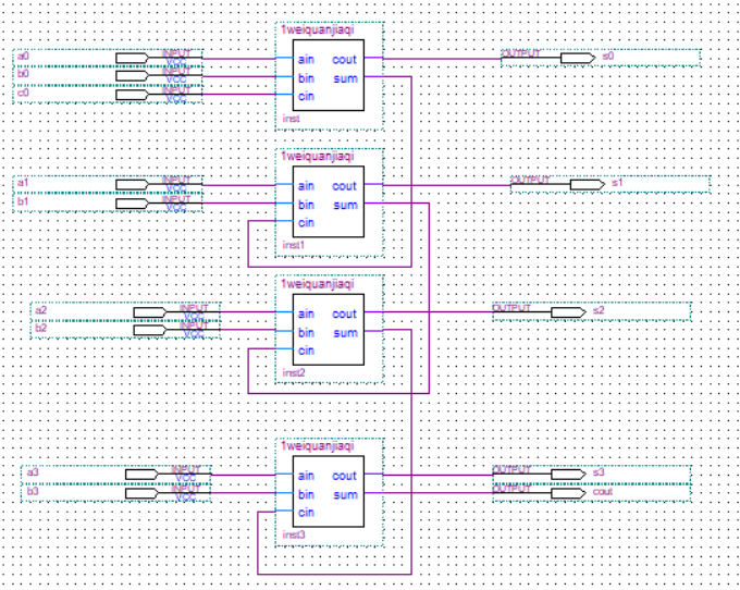
VHDL
-- 引入IEEE标准库,并使用std_logic_1164和std_logic_unsigned包。
-- std_logic_1164包定义了标准逻辑类型和操作。
-- std_logic_unsigned包提供了无符号数的算术运算。
LIBRARY IEEE;
USE IEEE.STD_LOGIC_1164.ALL;
USE IEEE.STD_LOGIC_UNSIGNED.ALL;

-- 定义实体ADDER4B,包含输入和输出端口:

ENTITY ADDER4B IS
 PORT (
 CIN4 : IN STD_LOGIC;  -- CIN4:输入进位,类型为std_logic。
 A4 : IN STD_LOGIC_VECTOR(3 DOWNTO 0);  -- A4和B4:两个4位输入二进制数
 B4 : IN STD_LOGIC_VECTOR(3 DOWNTO 0);
 S4 : OUT STD_LOGIC_VECTOR(3 DOWNTO 0); -- S4:4位输出和
 COUT4 : OUT STD_LOGIC                  -- COUT4:输出进位
 );
END ADDER4B;

 -- 定义架构behav。
ARCHITECTURE behav OF ADDER4B IS
 SIGNAL SINT : STD_LOGIC_VECTOR(4 DOWNTO 0); --用于存储加法运算的中间结果,包括进位。
 SIGNAL AA, BB : STD_LOGIC_VECTOR(4 DOWNTO 0); --用于存储扩展后的输入A4和B4。
BEGIN
 AA <= '0' & A4;  -- 将A4和B4扩展为5位,最高位填充0,分别赋值给AA和BB。
 BB <= '0' & B4; -- 这样做是为了在加法运算中包含进位。
 SINT <= AA + BB + CIN4;  -- 将AA、BB和CIN4相加,结果赋值给SINT。由于AA和BB都是5位,所以加法运算的结果也是5位。
 S4 <= SINT(3 DOWNTO 0);
 COUT4 <= SINT(4); -- 将SINT的低4位赋值给S4,最高位赋值给COUT4。

END behav;
-- 结束架构behav的定义。Code language: PHP (php)
N位全加器
library ieee;
use ieee.std_logic_1164.all;
-- 引入IEEE标准库和标准逻辑1164库

entity cla_addern is
 generic(n:integer:=8); -- 改变 n 可以设计任意位数全加器。
 port(
   in1, in2: in std_logic_vector(n-1 downto 0); -- 输入端口 in1 和 in2,n 位宽的标准逻辑向量
   carry_in: in std_logic; -- 输入进位信号
   sum: out std_logic_vector(n-1 downto 0); -- 输出端口 sum,n 位宽的标准逻辑向量
   carry_out: out std_logic -- 输出进位信号
 );
end cla_addern;
-- 定义一个可配置位数的超前进位加法器实体

architecture rtl2 of cla_addern is
 signal y, c: std_logic_vector(n-1 downto 0);
 -- 定义内部信号 y 和 c,n 位宽的标准逻辑向量
begin
 y(0) <= in1(0) xor in2(0) xor carry_in;
 -- 计算第0位的和,使用异或操作
 c(0) <= (in1(0) and in2(0)) or (in2(0) and carry_in) or (in1(0) and carry_in);
 -- 计算第0位的进位,使用与或操作

 gen: for i in 1 to n-1 generate
 -- 生成器语句,用于生成第1位到第(n-1)位的和和进位
 begin
   y(i) <= in1(i) xor in2(i) xor c(i-1);
   -- 计算第i位的和,使用异或操作
   c(i) <= (in1(i) and in2(i)) or (in2(i) and c(i-1)) or (in1(i) and c(i-1));
   -- 计算第i位的进位,使用与或操作
 end generate;

 sum <= y;
 -- 将内部信号 y 赋值给输出端口 sum
 carry_out <= c(n-1);
 -- 将最后一位的进位信号赋值给输出端口 carry_out
end rtl2;
-- 定义超前进位加法器的结构体Code language: PHP (php)


评论